TSMC, ASML look ahead to 3nm and 2nm chips
But companies like TSMC and Samsung won’t even have time to pat themselves on the back over their 5nm components. That’s because both foundries are already working on the 3nm process node. Back in 1965, Intel co-founder Gordon Moore observed that the transistor density on a chip doubled every year. He later revised that to a doubling of transistor density every other year. So that leaves little time to celebrate.
One of the tools developed to keep Moore’s Law alive is extreme ultraviolet (EUV) lithography. Lithography is used to print circuits on thin slices of silicon. When you think about the size of a chipset and the billions of transistors that need to be placed inside it, you can understand that extremely thin markings need to be made inside a chip. EUV uses ultraviolet beams to make this possible. The N5 node that TSMC is working with can use 5nm for up to 14 layers. The 3nm process node could deliver up to a 15% hike in power at the same transistor count as 5nm, and up to a 30% reduction in power use (at the same clock speeds and complexity).
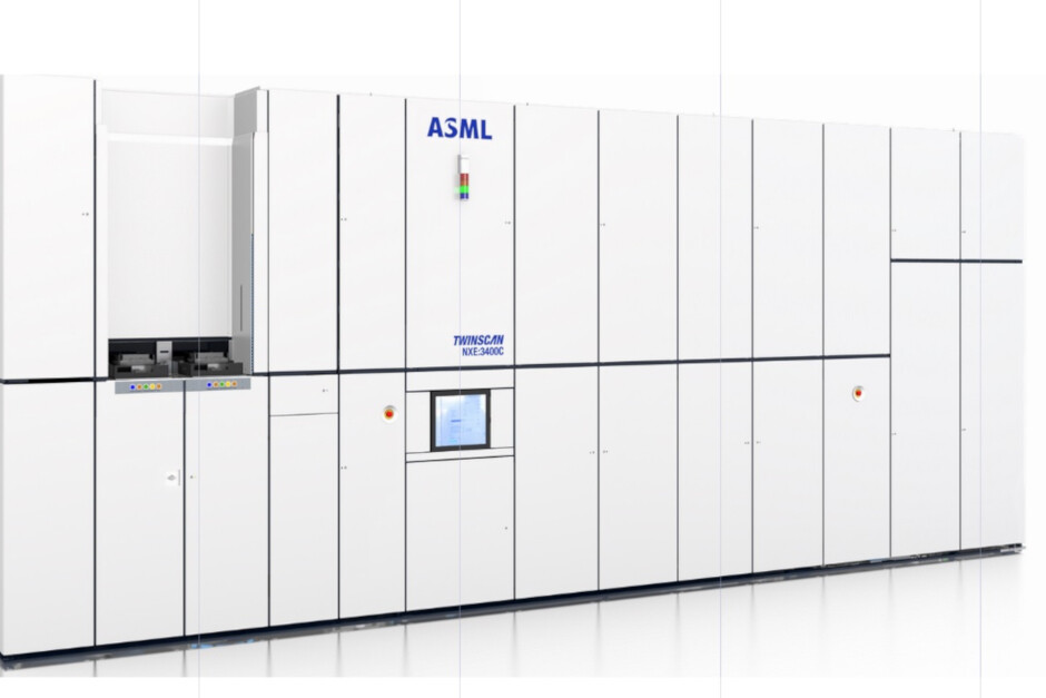
Dutch lithography company ASML says that at 3nm, lithography can be used on more than 20 layers. Peter Wennink, CEO of ASML, says that “I think, on the N5 in logic we are over 10 layers and in N3 we will be over 20 and we actually see that creeping up. That has just the fact that it gives so much more advantage to go to single patterning and take away these multi patterning DUV (Deep ultraviolet) strategies, which is also true for DRAM.” When a single lithography exposure does not produce a sharp resolution print, double patterning exposures are used. Memory (RAM and NAND) chip manufacturers rely on this process.
TSMC plans on using FinFET transistors for its 3nm mode before switching to GAAFET (gate all around) for 2nm chips. Unlike FinFET, which doesn’t surround a channel on all sides, GAA surrounds a channel using a Gate. The latter method makes current leakage almost negligible.

