The lower the process node, the smaller are the transistors used with a chip meaning that the transistor count can be higher. Typically the higher the transistor count, the more powerful and energy-efficient a chip is. There is one company in the world, Dutch firm ASML, that makes EUV machines and it has been promoting and selling the next-gen device. This is called the high-NA EUV machine and thanks to a hike in the numerical aperture to .55 from .33, more precise patterns can be etched on wafers that will be used to produce chips using the 2nm process node and lower.

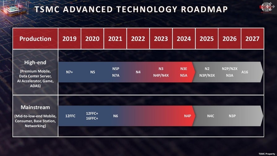
TSMC’s roadmap. | Image credit-TSMC
“The roadmap you see here is pretty much the same, actually it is the same technology roadmap that I think you saw during the [technology] symposium six months ago. We have N2, N2P, which is coming [to] productions next year and the year after. And then [they are] followed by A16.”-Dan Kochpatcharin, Head of Design Infrastructure Management, TSMC
The A16 uses a backside power delivery network (BSPDN) that moves the wires and connections that feed a chip with power from the front of the chip to the back which will improve performance efficiency.

