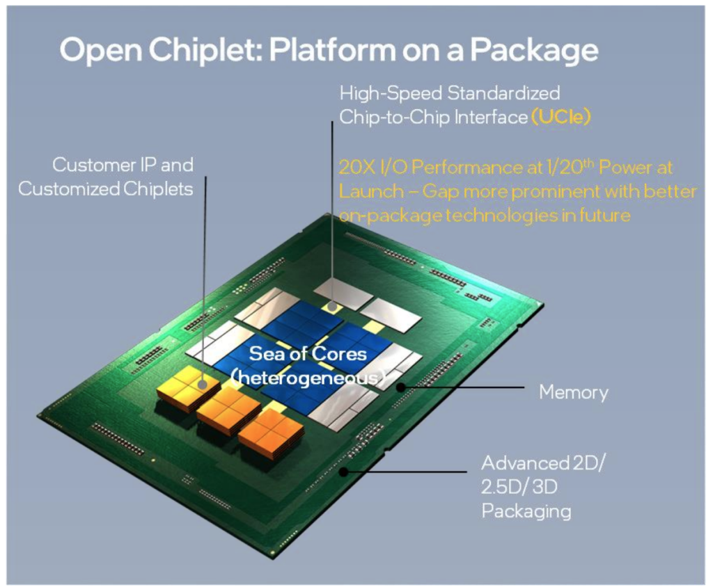
For years, the PC industry has embraced the mixing and matching of processors, expansion cards, memory, and more, all to create a modular, expandable platform. Now, a group of companies wants to do that at the chip level in what’s called Universal Chiplet Interconnect Express, or UCIe.
UCIe takes the concept of “chiplets”—individual pieces of self-contained logic, stitched together inside of a chip package—and opens it up to the semiconductor industry at large. Both AMD and Intel have done this for years: Intel with its co-EMIB and ODI connections, for example, which gave the world its hybrid chip, Alder Lake. A specialized engineering partnership between AMD and Intel also produced an Intel CPU that included an AMD GPU, called “Kaby Lake G“.
Enter UCIe, which is designed to make a future “Kaby Lake G” chip even easier to manufacture. UCIe transfers data using either the existing PCI Express standard or the related CXL (Compute Express Link) interface used by data centers. Essentially, a chip maker could take a CPU core from one company, a graphics core from another, and a WiFi radio or 5G radio front-end from a third chip company, and snap them together like LEGO blocks using UCIe, in much the same way you can drop a graphics card or an SSD into a PC’s PCI Express slot. With UCIe, this would simply be done at the chip level. (A UCIe white paper (PDF) has more.)
The membership of UCIe backers includes a who’s who of major chip and foundry vendors: AMD, Arm, Advanced Semiconductor Engineering, Inc. (ASE), Google Cloud, Intel, Meta/Facebook, Microsoft, Qualcomm, Samsung and TSMC. The exception? Nvidia, which has yet to formally sign on.
The new standard is also a concession of sorts, one that acknowledges the demands of today’s designs simply exceed the industry’s ability to physically manufacture them. For decades, the PC industry has tried to design all-in-one PC processors that contain a CPU, GPU, I/O, and more, all on a single chip. But larger and larger chips provide more opportunity for lithography errors that can render the entire chip worthless. Indeed, UCIe is built to anticipate the day when new, hybrid chips might simply be too physically large to manufacture using today’s lithographic equipment.
“What we’re seeing is that a lot of our designs are hitting the reticle limit as the demand for processing is insatiable, so it’s easier for us—and by ‘us’ I mean the broader industry—to build smaller chiplets and stitch them together on the package so that they act as a single entity,” UCIe chair and senior Intel fellow Debendra Das Sharma told HPCWire. “So this is a scale up kind of solution.”
Hypothetically, UCIe would mean that essentially anyone with the appropriate licenses and intellectual property could snap together a chip package containing logic from any number of companies. UCIe also suggests that any number of small startups could develop specialized logic, package them up with a UCIe interface, and sell them to other chip companies.
To be fair, the chip industry has already had this capability for decades, with programmable logic and FPGAs from companies like Altera and Xilinx—both recently acquired by Intel and AMD, interestingly enough. Which leads to an interesting speculation: In a decade or so, could Intel and AMD become the new “PC” builders?
As PCWorld’s senior editor, Mark focuses on Microsoft news and chip technology, among other beats. He has formerly written for PCMag, BYTE, Slashdot, eWEEK, and ReadWrite.

