TSMC negotiating to build a new fab in Singapore to alleviate the global chip shortage
The report from The Journal says that TSMC has not yet made a final decision about proceeding with a new fab and the factory being built in the U.S. (in the state of Arizona) is currently delayed. A new plant in Singapore would cost billions of dollars and some of the money to build the facility could come from the Singapore government. Those in the know say that TSMC is currently in negotiations with the country’s Economic Development Board.
Render of TSMC’s Arizona fab that is now being delayed
For example, the A13 Bionic chip powered the iPhone 11 series was built by TSMC using its 7nm process node. The chip contained 8.5 billion transistors. Compare that with the A15 Bionic chip built by TSMC using its 5nm process node. That chip, used on the iPhone 13 line, carries 15 billion transistors allowing it to be more powerful and energy-efficient than older chips.
Ironically, during the current global chip shortage, it has been these older legacy nodes that have been in short supply and have risen the most in price. But building fabs in other countries could help TSMC remain close to its major customers and is a way around some of the travel restrictions that come companies have imposed due to COVID. Last year Global Foundries announced that it would spend $4 billion to build a fab in Singapore that would open in 2023.
Singapore is responsible for 5% of global wafer fabrication
Singapore is already home to several chip suppliers as it has a large talent pool that these companies can choose from, and it has a strong supply chain. U.S. chipmaker Micron Technology, Germany’s Infineon Technologies, and Global Foundries have facilities in the country. The country’s trade and industry minister Alvin Tan said in January that semiconductors are “the fastest-growing segment of the electronics industry.”

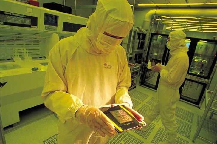
TSMC employee checking things out in a fab
Earlier this year, back in February, the world’s fourth-largest contract chip manufacturer, Taiwan’s United Microelectronics Corp., said that it would spend $5 billion to expand its production in Singapore. The latter country is home to 5% of global wafer fabrication capacity. Wafers are made of silicon and through various techniques they are turned into an ingot. The ingots are then sliced into thin discs called wafers on which extremely thin circuity patterns are etched in a process known as lithography.
After being polished to a mirror finish, the wafers go through several stages and cut into dies. They are then tested, packaged, and shipped.

