
The larger the number of transistors that fit in a square mm space, the more powerful and energy-efficient that chip is. From the 7nm process node used on the A11 Bionic and Snapdragon 865 to the 2nm node that IBM is writing about, the performance increase amounts to 45% using the same amount of power. That works out to a 75% power savings at the same power level.
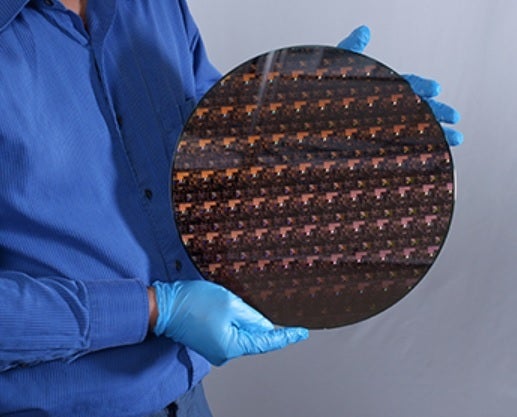
Chips are cut out of wafers like the 11.8-inch wafer used for 5nm chips
To help cram billions of transistors inside a chip, IBM uses Extreme Ultraviolet Lithography (EUV), which produces lines smaller than visible light. These lines create the patterns that will be used to create circuits. IBM also replaced the FinFET architecture with GAA and as IBM puts it, “Four “gates” on a transistor enable superior electrical signals to pass through and between other transistors on a chip.”
And for those worried that we’re coming to the end of Moore’s Law (the observation made by Intel co-founder Gordon Moore that the transistor density in chips doubles every other year), IBM Research says that it “continues to explore options for continued scaling to 1nm and beyond.” IBM says that it is still several years from manufacturing its 2nm node devices and that this year it will debut its first commercialized 7nm processor. Next year, TSMC and Samsung Foundry are expected to begin volume production of chips using the 3nm process node.